Products
VCSEL
Vertical-cavity surface-emitting lasers, characterized and qualified in-house. This is the one area where we publish performance results and where product is available today.
Readout
Wavelength vs. temperature
The scale below is the wavelength axis itself: the fine dots are the scale, now sized to the band our devices actually occupy rather than a supplier catalogue. Characterized samples — etalon read at 791.5 nm, 25 µm mesa, 3 µm aperture — were swept on a WaveEye wavelength meter from 24.07 °C to 30 °C, moving 791.035 nm to 791.315 nm. The rubidium D1 line those atomic sensors need sits at 794.98 nm, marked as the target the tuning is aimed at.
Characterization and test
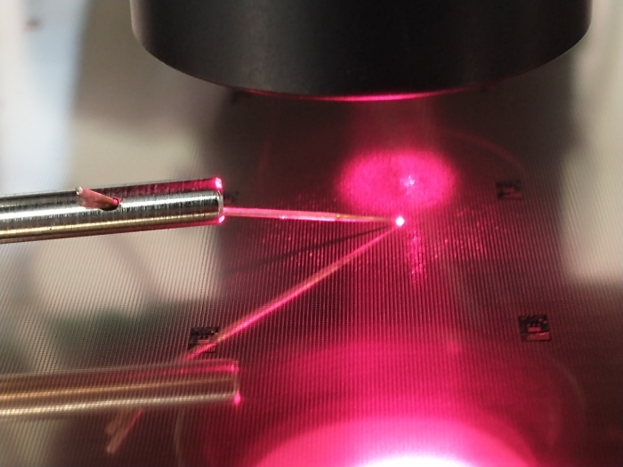
A laser is only as useful as the record that comes with it. Every die is probed on an automated test and scan setup built in-house, because the equipment to do it at the precision atomic sensing needs was not available to buy. That setup is what turns VCSEL characterization from a bench process into a repeatable one.
The same discipline runs through the rest of the work: parts are qualified before they leave, results are recorded per die rather than per batch, and what we publish about a part is what we measured on it. Detailed performance data is shared directly with customers evaluating a design-in.
A separate high-power multijunction line targets 905 nm and 940 nm for automotive applications, built and qualified on the same in-house test and scan setup.
Related
Metasurface work is developed alongside these devices. See Products for the wider set, or Capabilities for the systems this technology sits inside.